
Author

Disclaimer. This article is for informational purposes only and is not intended to instruct or encourage any illegal activity. Our goal is to describe the existing vulnerabilities that can be exploited by attackers, to warn users, and to provide recommendations on how to protect their personal information online. The authors are not responsible for how the information is used. Remember to always prioritize the security of your personal data.
When developing hardware solutions based on microcontrollers (MCUs), manufacturers seek to protect their firmware from falling into the hands of attackers, because it may contain sensitive information, encryption keys, unique valuable algorithms, and so on. To achieve this, most microcontrollers implement flash memory readout protection technologies. But do they really provide sufficient protection?
Unfortunately, no. Not all readout protection technologies work as intended. Vulnerabilities in debug interfaces, non-trivial fault injection attacks, and even invasive tampering can be exploited to bypass the protection.
At Positive Labs, we conduct security research on a wide variety of hardware. So when a device based on GigaDevice’s GD32 microcontroller fell into our hands, we found ourselves investigating its protection technologies before we knew it. GD32 microcontrollers are quite popular and are used everywhere, including as replacements for STM32 microcontrollers, as they are often pin-compatible and even share the same memory address map. The research turned out to be quite fascinating, and the results were impressive!
Readout protection: what is it and how it works
Readout protection technologies go by different names. For example, STMicroelectronics calls it Readout Protection, or RDP, in nRF microcontrollers it’s known as APPROTECT; and for GigaDevice it’s called Security Protection. Further in this article, we will talk about Security Protection, but we will use the name Readout Protection (or RDP) because it is more widely used and best conveys the essence of the technology.
The operating principles of these technologies are very similar, despite their different names. All of these technologies implement multiple protection levels, each imposing its own restrictions:
- RDP0 (level 0, no protection). No restrictions are imposed. In this state, microcontrollers are delivered to developers — they can be freely programmed and debugged.
- RDP1 (level 1, low protection). At this level, access to flash memory is blocked when a debugger is connected. However, the contents of the SRAM generally remain accessible for reading and writing via the debugger. This level can be downgraded, but doing so will erase the flash memory contents. For some microcontrollers, this level of protection is the maximum available.
- RDP2 (level 2, high protection). At this level, the debug interface is typically permanently disabled, and the possibility of booting via the built-in bootloader (used for programming) and accessing the SRAM is also disabled. As a result, the ability to interact with the microcontroller or influence its execution is significantly reduced. Moreover, this level cannot be downgraded, meaning the microcontroller cannot be repurposed for other uses.
Usually, the current protection level is determined by the value of a specific byte that is physically stored in the same flash memory cells (in the Option Bytes area) where the microcontroller firmware is located, but the method of programming this byte varies.
Before moving on, it’s worth talking about some known techniques for bypassing readout protection on various microcontrollers. This will help understanding the general approaches available. Moreover, some well-known techniques have proven useful and were applied in our research. In our opinion, to fully immerse oneself in the topic, one should review the two studies by Johannes Obermeier and his co-authors, along with related materials. Below is an overview based on them.
Shedding too much light on a microcontroller’s firmware protection
Here you can find a Johannes Obermeier’s STM32F0 research. In this research, three techniques are described: Cold-Boot Stepping (CBS), RDP2 downgrade and exploitation of debug interface vulnerabilities.
As we noted before, at the low level (RDP1), a SRAM content is typically accessible. During development, it’s necessary to take this into account and try to clear the SRAM contents of secrets as soon as possible. In some cases, however, even this will not suffice. The Cold-Boot Stepping (CBS) technique allows one to obtain a set of intermediate SRAM states with high precision—even down to the state after each instruction.

Source: https://www.aisec.fraunhofer.de/en/FirmwareProtection.html
For example, the researchers describe a case where firmware integrity is verified using the CRC32 algorithm. By intercepting all intermediate CRC32 values with the CBS technique, it is possible to fully reconstruct the firmware content.
The second technique is an example of an invasive attack that requires access to the chip’s internals. The researchers used acid to gain access to the crystal inside the microcontroller. By exposing memory cells to ultraviolet rays of a specific wavelength, they were able to alter the byte responsible for the protection level. As a result, the protection level was reduced from RDP2 to RDP1. This attack is quite complex, as it requires the researcher to have knowledge of chemistry, memory cell physics, and crystal structure, and the process of etching the chip’s package should ideally be performed in a specialized laboratory.

Source: https://www.aisec.fraunhofer.de/en/FirmwareProtection.html
The last technique demonstrated in the research exploits a vulnerability via the debug interface at RDP1. The researchers found that flash memory locking occurs upon the first access to the bus via SWD, and if that access is a flash memory read, there is a chance to obtain the read result. For the exploitation, the researchers used a different STM32 microcontroller as the attacking device. There are ported projects available for alternative microcontrollers (for example, RP2040). Additionally, note that the attack works on some other microcontrollers (not only STM32). If an attack board is not available to implement the attacking device, one can make do with a J-Link paired with OpenOCD and a software-controlled relay.
Thus, the researchers demonstrated that the protection of the STM32F0 can be completely bypassed regardless of the set RDP level. The attack on RDP1 is very easy to implement, which cannot be said for the invasive attack on RDP2.
One exploit to rule them all? On the security of drop-in replacement and counterfeit microcontrollers
The research itself and its materials can be found here.
The main focus of the research was on the STM32F1 microcontrollers and its clones, including those from GigaDevice. The research demonstrates various techniques for bypassing RDP1 via the debug interface, an invasive attack on RDP2, and a voltage glitch technique to bypass RDP1. More details on each method can be found in the original source. For now, we will only discuss those most critical to our research.

Source: https://gd32mcu.com/data/documents/datasheet/GD32F103xx_Datasheet_Rev2.12.pdf
Access to the flash memory controller (FMC) can be gained through various means as shown in the block diagram above: the core has direct access to the FMC via the instruction and data buses. In addition, the FMC is connected to the AHB bus, and the bus master devices (the core, DMA engine) can initiate flash memory operations. Many well-known attacks are possible because not all of these methods of accessing the flash memory are accounted for when the lock is activated. In some microcontrollers, RDP1 does not block the core’s access via the instruction and data buses, which allows the flash memory content to be obtained using load instructions. Sometimes, only access via the instruction bus remains possible, in which case a security researcher can retrieve the flash memory contents by manipulating the vector table offset register (VTOR) and manually triggering various interrupts, as detailed in the “Exception(al) Failure — Breaking the STM32F1 Read-Out Protection” research. In the case of the GD32F103, the possibility of an attack by copying the flash memory content into SRAM via the DMA engine using a debugger is demonstrated. The idea of using the DMA engine proved useful in our research when exploiting one of the vulnerabilities.
Let’s take a look at the invasive attack on the GD32F103/GD32F130 chips. In this attack, the researchers exploit the microcontroller’s multi-chip structure.

Source: https://we.easyelectronics.ru/STM32/cs32f103c8t6-gd32f103cbt6-i-drugie-kitayskie-klony-stm32f103c8t6-i-stm32f030c8t6.html#cut

Source: https://www.usenix.org/system/files/woot20-paper-obermaier.pdf
As shown in the diagram, the microcontroller consists of a logic crystal and a flash memory crystal, connected by bonding wires, which can be accessed using a polishing sheet. In our opinion, this is simpler than the chemical decapsulation described earlier, but it still requires certain skills. The researchers discovered that the flash memory communicates using the QSPI protocol, through which, after a power-on reset, the following are read: factory configuration, built-in bootloader, Option Bytes, and part of the firmware. The read data is apparently cached for faster access later. This information about the primary initialization process also proved very useful. Based on this, we were able to make some assumptions about how the vulnerabilities we discovered operate at a lower level.

Source: https://www.usenix.org/system/files/woot20-paper-obermaier.pdf
Finally, let’s talk briefly about fault injection attacks. It seems that, along with invasive attacks, these are the last resort for a potential attacker to bypass readout protection, especially in RDP2, when the debug interface is inaccessible and the attack surface is considerably reduced. In the discussed work, the researchers managed to use a voltage glitch to reset the flash memory lock state after connecting the debugger, while not losing the pre-prepared SRAM content needed for subsequent attack stages. This attack targets RDP1, but there are numerous successful examples of lowering RDP2 and enabling the debug interface using voltage glitches:
- nRF52 Debug Resurrection (APPROTECT Bypass). An example of bypassing the APPROTECT technology in nRF52 to gain access to the debug interface and flash memory.
- wallet.fail — Hacking the most popular cryptocurrency hardware wallets. This research examines the security of popular crypto wallets and various attacks against them. One of the cases is the Trezor wallet based on STM32F2/4. By applying a voltage glitch, the researchers successfully lowered the RDP2 level and accessed the debug interface.
- chip.fail — Glitching the silicon of the Internet-of-Things. The research is dedicated to using voltage glitches on various microcontrollers, including lowering protection levels and enabling the debug interface.
In summary, there are three main approaches for bypassing RDP technologies can be highlighted:
- Attacks via the debug interface: relevant when the debug interface is accessible (for example, in RDP1) or when it has been already activated through other attacks.
- Fault injection attacks in general, and voltage glitches in particular: effective attacks that can often be implemented without expensive tools, although they may require extensive pre-research to find the correct attack parameters.
- Invasive attacks: complex attacks that require specialized equipment and skills, but in some cases can be carried out with improvised materials.
Finally, we move on to our research and the vulnerabilities we discovered. Two of them allow using the debug interface even if RDP2 is enabled and, depending on the microcontroller family, to obtain either a snapshot of the SRAM or the complete flash memory content.
How it all began
The research began with the study of an air quality sensor. The device was based on the GigaDevice GD32E230 ARM microcontroller. We were particularly interested in the firmware protection of the sensor and decided to investigate it. On the PCB, there was a SWD debug interface and NRST, VCC, and GND pins.
At first, we attempted to connect via SWD using J-Link—and we were surprised. Debugging didn’t work with the official J-Link utility, but we managed to read the Debug Port Identification Register (DPIDR). Even OpenOCD with a specific configuration for the microcontroller couldn’t handle this initially. Using a logic analyzer, we discovered that the J-Link utilities attempted various connection methods, including connecting during reset by pulling the NRST signal to ground. After realizing this, we modified the OpenOCD configuration and through some experiments achieved a similar result as with J-Link—the DPIDR was successfully obtained, although debugging still did not function properly. The observed behavior was unusual, and while we couldn’t successfully start debugging, we were not sure that the chip was locked in RDP2. It could just be a simple SWD pin misconfiguration.
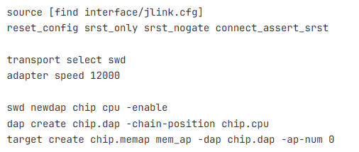
We attempted to explore SWD capabilities in the microcontroller’s reset state. For this purpose, we made an OpenOCD configuration where NRST was pulled to GND during connection. Additionally, the NRST signal could be freely controlled:
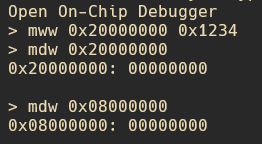
We found that reading and writing to various addresses on the bus was possible, but the results of the operations did not always meet expectations. For example, writing a value to SRAM and reading it resulted in zeroes. Similarly, reading flash memory consistently returned zeroes:
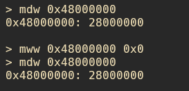
When attempting to read different peripherals, reset values were obtained as described in the user manual, as expected. However, these values could not be changed:
Debug modules presented more interesting outcomes: they were not in reset state and could be configured. For example, setting the CDEBUG_EN bit in the Debug Halting Control and Status Register (DHCSR) required specifying the correct key in the register’s upper bits. Additionally, writing to the comparators of the Flash Patch and Breakpoint (FPB) module worked as intended.

Using the debug modules, we explored ways to halt the core upon startup, but SWD was still inaccessible. This was likely due to RDP2, but to confirm this conclusively, it was decided to procure an identical clean chip, flash it with our firmware, and see if RDP2 locking was possible.
Upon testing, the behavior of our RDP2-locked chip matched that of the target device. It can be definitively stated that RDP2 is active, which means that extracting the firmware via SWD is not possible. But the availability of the debug interface during reset was seemed very strange to us. Referring to the STM32 microcontroller documentation, it states that with RDP2 enabled, the debug interface is disabled even during reset. This is not the case with GD32, and we decided to investigate this microcontroller’s unique characteristics.
GigaVulnerability #1
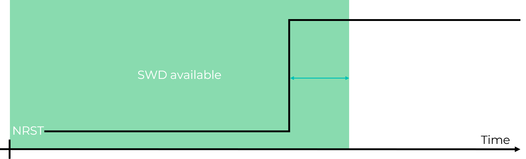
The idea for the first potential vulnerability was quite obvious. As we discovered, the SWD interface is accessible in the reset state. It is possible that after exiting the reset state, some time is required to disable SWD, and this race window (the moment when SWD remains available after the reset signal state changes) could be exploited to access the bus. This can be illustrated schematically as shown in the figure:
To check if this vulnerability can be realized, we first need to understand a little bit about how SWD is structured. Its detailed description can be found in the Arm Debug Interface Architecture Specification. In this article, we will provide a concise overview of the key aspects necessary for vulnerability verification. Two signals are used in in the protocol:
- SWCLK: clock signal
- SWDIO: data input/output signal
Using these signals, it is possible to transmit specific packets for reading or writing registers in the debug port (DP) or access port (AP).

Source: https://documentation-service.arm.com/static/5f8ff91cf86e16515cdbfdf0

Source: https://documentation-service.arm.com/static/5f8ff91cf86e16515cdbfdf0
Physically, the debugger connects to the DP, through which access to various memory banks within one or multiple APs can be obtained.

Source: https://documentation-service.arm.com/static/5f8ff91cf86e16515cdbfdf0
In the DP, four registers can be accessed by their addresses, but depending on the type of operation, different registers may be available at the same address.
| Address | Read | Write |
|---|---|---|
| 0x00 | IDCODE | ABORT |
| 0x04 | CTRL/STAT | CTRL/STAT |
| 0x08 | SELECT | |
| 0x0c | RDBUFF |
The IDCODE register is the DP identifier—the value we attempted to retrieve using J-Link and OpenOCD. As mentioned earlier, there can be multiple APs, and each AP can have more than four registers. The SELECT DP register is required to choose the appropriate AP and the register bank within it. Reading AP registers occurs with a one-operation delay: the first read returns an undefined value, the second read returns the result of the first operation, and so on. The RDBUFF DP register is used to retrieve the result of the last AP register read without initiating a new operation.
The ADI specification defines three power domains—groups of chip components whose power supply can be controlled independently:
- Always-on power domain: consists of components that must always remain powered, such as the DP
- System power domain: consists of system components
- Debug power domain: consists of debugging components
Control over the system and debug power domains is managed using the four most significant bits of the CTRL/STAT register: CTRL bits request power domain activation, while ACK bits confirm the activation of the selected domain.

Source: https://documentation-service.arm.com/static/5f8ff91cf86e16515cdbfdf0